Full speed AVR based Graphics LCD Controller
for Optrex DMF-50840 display
Graphics LCDs are now available for hobbyists, both B/W and color, but a lot of them have no controller, meaning they have to be provided with constantly repeating line data. This is a full-time job, even for AVRs. On top of that, the information to be displayed on the screen has to be stored in RAM memory, and requires a lot more than the small amount of RAM available on most microcontrollers.
The Optrex DMF-50840 is a monochrome QVGA (320 x 240) LCD display with NO controller. It has a 4 bit (nibble) data interface, the usual DotClk, HSYNC, VSYNC lines plus an Enable line. Power requirements are +5V (Vcc), -26V (Vee, aka LCD Bias) and a contrast adjustment input (Vadj), somewhere around -20V. The input cable is a 14-pin FFC, with a pitch of 1.25mm. This cable (soldered to the LCD) mates with a Molex 39-53-2144 FFC/FPC connector, which I soldered to a DIP adapter to use on the breadboard based controller. For the more permanent controller (as shown in picture), I used a Molex 52044-1445 FFC/FPC connector. Both connectors are through hole.
The good news is that this display does not need the common "M" input, an oscillating input needed to prevent the LCD crystals from being operated in DC mode. The bad news is that, once the Enable line is set High, the timings lines need to be constantly toggled to prevent the same damage when Vee is connected (-26V LCD Bias voltage). This means that no ICE debugging can be done while Vee/Vadj are connected. Unplug the Vee/Vadj lines when using the Jtagice mkII!
This display has the usual CCFL backlight, which requires an inverter.
The controller design.
The task of an LCD controller is to send one line of data to the LCD, toggling the DOTCLK line for every nibble, then toggle the HSYNC signal, which forces the LCD to show this one line on the screen and to prepare for the next line of data. Once all lines are sent, the VSYNC signal needs to be toggled, indicating that the LCD needs to start at the top of the screen for the next line of data. Doing this fast enough will create the illusion to our eyes of a stable image. It is the same principle as the raster scan method used in CRT video display and TV. At the same time, the controller must provide an interface to the outside world to allow useful information to be sent to the display, so that there is something to show (the user interface).
QVGA resolution is 320 horizontal by 240 vertical. Since the horizontal input is done 4 bits at a time, we need to toggle 320 / 4 = 80 nibbles per line. To do one frame, we need 240 * 80 = 19,200 nibbles.
This LCD does not require any overscan. Overscan is a left over from the old CRT designs, where the controller needs to provide extra time between lines and frames to allow the electron beam to move to the next location (beginning of next line or top of screen). Some other LCDs, for example the Sony ACX705AKM as used in the AVCX project, do require this overscan (according to the datasheet), which makes it harder for one microcontroller to do all the work (though not impossible).
To achieve a refresh rate of 60 Hz (progressive scan), we need to clock 60 * 19,200 = 1,152,000 nibbles per second. In this design, each nibble takes 4 cycles, which includes the DOTCLK toggling. There is also about 70 cycles overhead for each line (register setup, Hsync, sometimes Vsync, Enable). The total number of cycles required to refresh this display is thus 4 * 1,152,000 + 70 * (240 * 60) = 5,616,000 per second. For an AVR running at 20 Mhz, this means it's busy 28% of the time doing refreshes, leaving over 70% for other tasks, mainly to update the display memory based on external graphics commands from the user interface.
As mentioned, one frame requires 19,200 nibbles of memory, which equates to 9,600 bytes. Most AVRs don't have that much memory. Therefore an external SRAM chip is used to store the bitmap. I've used the Cypress CY7C199 SRAM chip, a 32K x 8 bit Static Ram chip, available from Digikey for about $2.00. This controller only uses the lower 4 bits of the SRAM chip and The SRAM data bus is directly connected to the LCD data bus. This means that the AVR doesn't actually need to read the SRAM data when refreshing; it only needs to make sure that the SRAM produces the correct bits on its data bus, is itself in high-Z state on that bus and properly clocks the DOTCLK line. Using the Read Cycle No. 1 method (CY7C199 datasheet page 5, change address only) and preloading 2 registers to control the DOTCLK, means that only 4 instructions (one cycle each) to clock one nibble into the LCD are needed:
|
out SRAMVX,r19 |
; Select Horizontal address, bits 0..6 |
|
inc r19 |
; update address, data now available |
|
out PC_OUT,PORTCCLKON |
; DOTCLK ON |
|
out PC_OUT,PORTCCLKOFF |
; DOTCLK OFF |
Note that the sbi and cbi instructions are not used here since they each require 2 cycles.
The refresh is done using Timer0, which is executed every 67.2 microseconds (14,880 Hz). At 240 lines per frame, we get 14,880 / 240 = 62 frames per second, producing a rock solid image. To optimize the refresh cycle count, the Timer0 ISR is written in AVR assembly, but everything else is written in C (Winavr).
It is very important to control the access to the SRAM precisely, since we need to update the SRAM constantly to actually make the LCD show something interesting. This is done by the function "WriteNibble":
void WriteNibble(uint8 data, uint8 x, uint8 y)
{uint8 CpuStatus;
CpuStatus = SREG; //save interrupt status
cli();
//
// only HSYNC and VSYNC relevant in lower 4 bits, which are always low here
//
SRAMDATAO = (data << 4);
SRAMVX = x;
SRAMVY = y;
cbi(SRAM_WE, WE_BIT);
sbi(SRAM_WE, WE_BIT);
SREG = CpuStatus; //restore interrupt status}
As you can see, the Data
Direction bits (DDR) are not set here since they are set to output at startup.
When the Timer0 ISR runs, it changes the DDR bits to input (which is the High-Z
state, effectively disconnecting the AVR from the data bus) before clocking in
one line, then changes them back to output. Once the SRAM update starts, no LCD
refresh can take place since that would modify the SRAM address access ports (SRAMVX,
SRAMVY), so we save the current CPU state and disable interrupts. The SRAM data
bus is connected to bits 4..7. Bits 0, 1 are used by the UART of the AVR so can
be ignored. Bits 2 and 3 are the HSYNC and VSYNC signals, which are normally
low, and only toggled when doing an LCD line refresh. Because interrupts are
disabled here, the refresh won't happen and we can write 0 values to these bits
without changing them; the line "SRAMDATAO = (data << 4)" will write 0 values to
the lower 4 bits since "data" is of type unsigned.
The use of an SRAM means that many address lines are required to control the SRAM chip, in this case 15. This means 15 I/O pins need to be dedicated; a 40 pin AVR just works; 28 pin AVR don't have enough port pins. It is possible to use a DRAM chip. which multiplexes the address lines. That saves 8 address pins. However more control pins are needed (RAS, CAS), gaining a net win of 6 pins. The drawback is that memory access is slower, since the memory address needs to be set in 2 steps. Using page mode during the LCD refresh will reduce this somewhat. In summary, for the fastest screen refresh rates, use an SRAM If you need to save port pins, use a DRAM. Keep in mind that the popular 28 pin AVRs (like the Atmega168) do NOT have a complete 8 bit port available to use as an address interface (when running with an external clock or crystal and using the Serial Port), requiring clumsy bit manipulation code.
The rest of the controller consists of an interrupt driven Serial handler, using a 512 bytes input buffer, a general purpose TC1 timer used for bookkeeping purposes and the main forever loop which pulls graphic command data from the input buffer, parses them and updates the SRAM memory accordingly. The controller will issue feedback if the input buffer has less than 50 bytes of free space, which could be changed to some form of software flow control. However, sending a full bitmap (9600 bytes) at 115,200 bps does not trigger this condition. The controller currently is capable of displaying text (8 x 8 font), monochrome images, arbitrary pixels and has DrawLine and DrawCircle primitives. The graphic command language is based on the AVCX command language. A PC based application, called AVCXaccess, is used to send graphic commands over the serial port to the controller at 115,200 bps. This application uses overlapped Serial port I/O so that both output and input can be handled simultaneously.
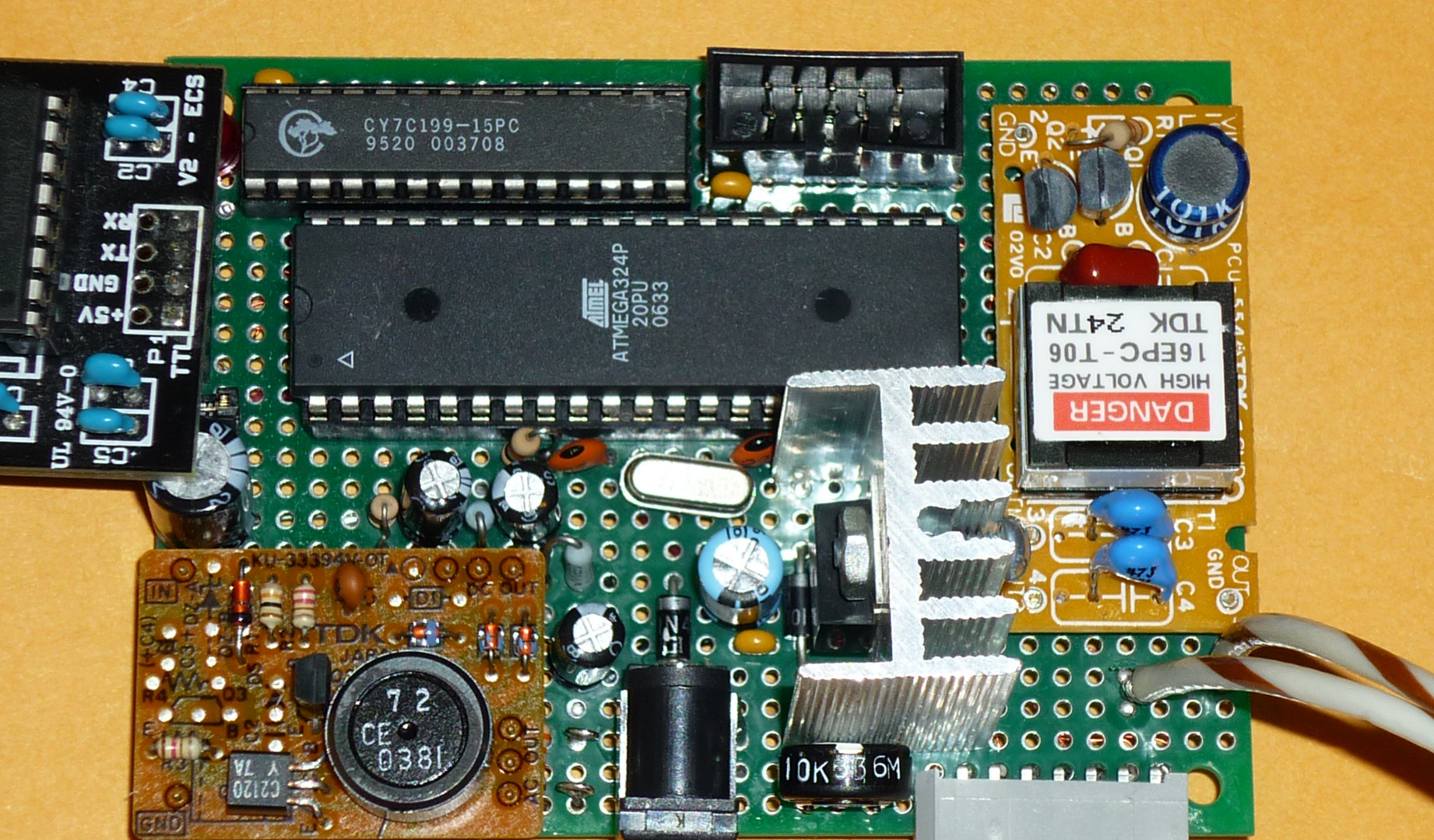
The Enhanced AVCX graphics command language is a byte stream of data, where most commands require more than 1 byte. Losing a byte will therefore disrupt the synchronization between the controller and the PC. A timeout mechanism is present to reset the graphics controller if no input has been received for 5 seconds. This controller is a simplification of a previous controller I built, the AVCX project (based on another design). That project uses 2 separate AVRs, is surface mount on a dedicated PCB and is all written in AVR assembly language. This DMF-50840 controller uses a 40-pin DIP AVR (Atmega324p), a 28 pin DIP SRAM chip, can be built on a breadboard and is mostly written in C. As a result, this project is much easier to implement and modify.
This implementation also has a built-in analog clock. The clock face uses 240 x 240 pixels, left aligned, leaving a pane of 60 x 240 pixels on the right side for other uses. The Enhanced AVCX graphics command language contains command to control the clock. No activity (meaning no incoming graphic control commands) for 1 minutes will also turn on the clock, as a screen saver.
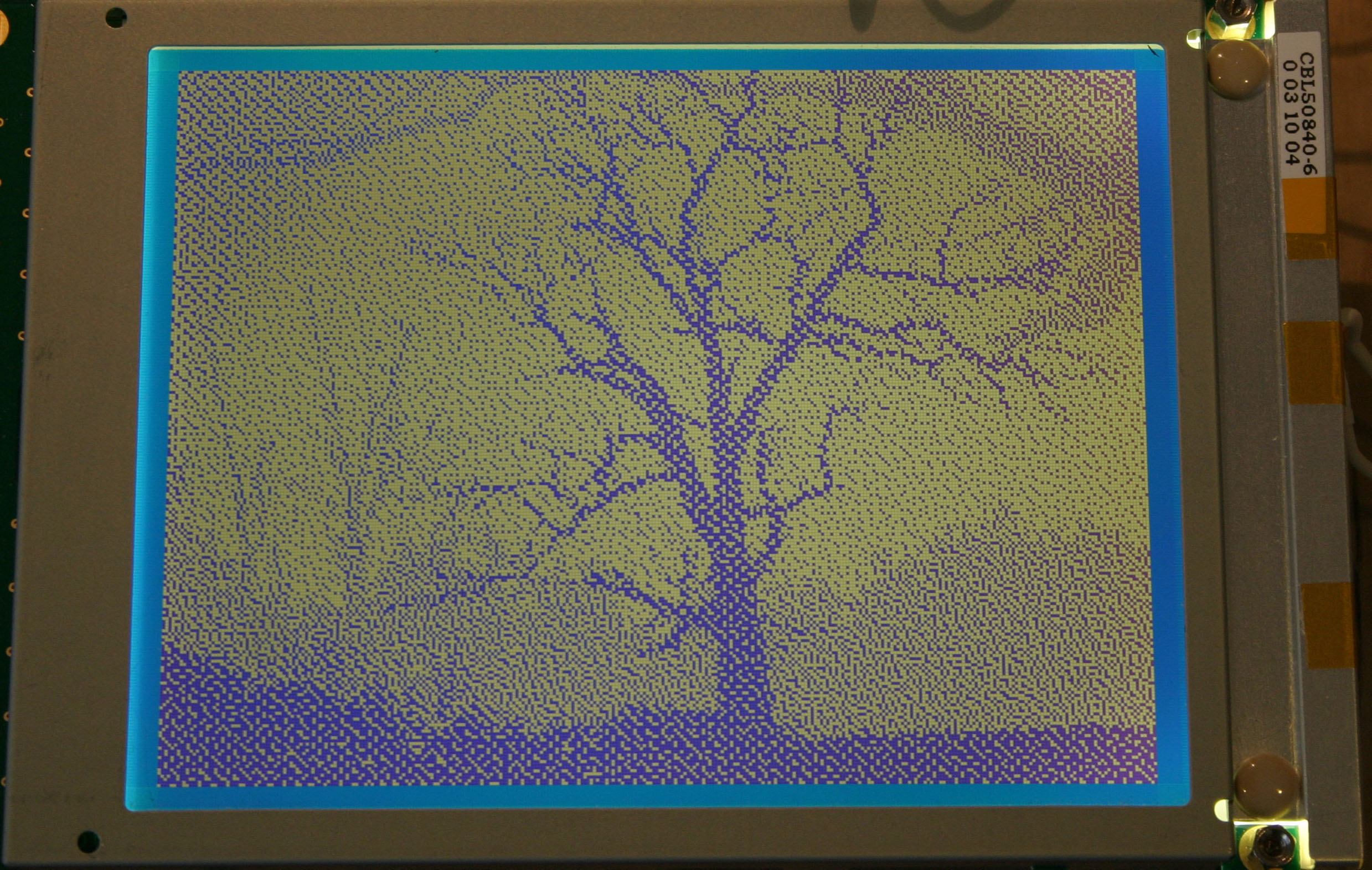
The initial version of this controller was built on a breadboard but was unreliable. Even though the LCD worked as designed, there were spurious pixels on the screen, caused by the SRAM memory being randomly set. Once I made the board version, as shown in the picture above, using point to point wiring, these problems disappeared.
Here are the connections:
Atmega324p connected to SRAM:
PA0..PA7: 8-bit Line address (Vy)
PB0..PB6: 7-bit horizontal address (Vx)
PC1: WE (Write Enable, active Low)
Atmega324p connected to SRAM and LCD:
PD4..PD7: Data bus (Data0..Data3)
Atmega324p connected to LCD:
PD2: VSync
PD3: HSync
PC6: DOTCLK
PC0: LCD Enable
Atmega324p other:
PD0..PD1: Serial Interface to PC
PC7: Debug Led
PC2..PC5: JTAG interface
PB7: n.c.
CY7C199 SRAM:
A0..A6: PB0..PB6 Vx
A7..A14: PA0..PA7 Vy
CE, OE: connected to GND
Data0..Data3: PD4..PD7 Data bus AND LCD connector pins 1..4
Data4..Data7: not connected
WE: PC0
LCD connector:
1..4: Data0..Data3
5: LCD Enable (PC0)
6: VSync (PD2)
7: not connected
8: HSync (PD3)
9: DOTCLK (PC6)
10: Vcc (+5V)
11: Vss (Gnd)
12: Vee (LCD Bias, -26V)
13: VAdj (potentiometer runner, ends at -26V and +5V)
14: Gnd
The DMF-50840 also requires High Voltage AC power to drive the CCFL backlight. For the initial breadboard version I used an Astec AA9090A series DC/DC converter from Hosfelt Electronics (item 40-206) which provides all the required voltages: +5V, -26V for the LCD Bias voltage and 350 VAC for the backlight. The board version uses a TDK inverter for the CCFL backlight (Electric Goldmine G16565) and an DC-DC converter (DC-32 from All Electronics) for the Vee supply. Both of these units have +5V inputs but require a lot of current (at least 0.5 Amp together). The board controller has a on-board +5V regulator which requires a heatsink for this reason. A more efficient version of the -26V supply is definitely possible, but I had this DC-32 board ready to use.
Please note that the Atmega324p fuse needs to be set to Full Swing External Crystal to operate reliably (I've learned that the hard way)
The user interface is currently driven by a demo application running on a PC. Communication with a PC requires the use of an RS-232 level converter. I used an external plug-in board for this. It is possible to use an FT232RL based USB-Serial adapter, however I found that such an adapter cannot be reliably used at speeds over 57600 baud.
Since development of the software for this controller is part of the fun, I wanted to have the ability to use the JTAGICE mkII hardware debugger. This requires that 4 pins (PC2..PC5) are reserved, limiting the potential enhancements of this controller. For example, an SPI interface would make the user communication faster. Driving this controller from another AVR board will be one of the next projects. It should be possible to run the serial interface at +5V levels (no level conversion) and at much higher speeds.
The PC based application "AVCXAccess" is a demonstration program on how to send graphics commands and data to the LCD-DMF50840 controller. The default is 115,200 at COM2 but is accepts 2 optional command line arguments for the COM port and the baudrate. Note that to change the baudrate, the controller software also has to be updated. A release build is included in the archive. The program will look for various bitmaps in the CURRENT directory so it needs to be started in the AVCXaccess directory like this: "Release\AVCXaccess.exe 1"; the optional '1' indicates that COM1: needs to be used.
Improvements:
The current user interface is an enhanced version of the AVCX protocol but it would be better to standardize the graphics interface to some industry standard. The SED1335 controller is the standard for monochrome 4-bit LCDs. The SED1335 provides an 8 bit parallel user interface, plus several control lines, including the A line indicating a command (as opposed to data). I have not seen a serial version of the SED1335 interface. Standardizing on an industry standard would make porting of existing software easier. Though not trivial, a serial version should be doable, even if not all features of the SED1335 can be implemented. One feature is the use of various planes, specifically a graphics plane and a text plane. I have looked into doing that for the current controller but found it impossible to do. Due to the lack of available memory (and AVR pins for larger memory chips), it would require that the planes be dynamically merged, meaning at refresh time, while the current SRAM memory would be reserved for the graphics plane (the internal AVR ram could be used for the text plane). The number of cycles needed for this dynamic merging exceed the available time, resulting in a very slow refresh rate. The Atmega1284P, if it ever becomes available, has 16KB internal memory, meaning that it can hold both one graphics plane as well as the text plane. The merged representation can thus be maintained in the SRAM chip (and be used directly for the screen refresh); any change in the graphics or text plane will be reflected in the merged representation immediately. One drawback of the SED1335 user interface is that it is completely byte oriented; no individual pixel access is available which means that any pixel set requires a GRAM read, followed by a GRAM write (unless the application itself maintains a frame buffer). The current Enhanced AVCX protocol has full support for pixel access.
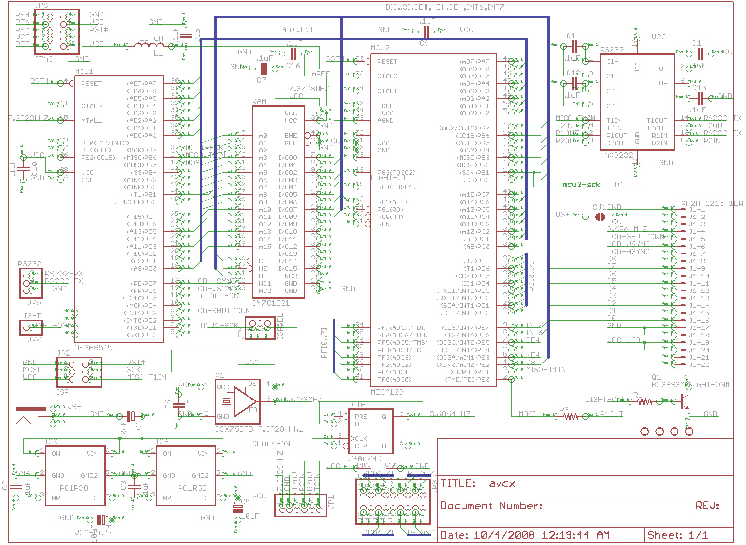
Here are the Schematics:
Here is what the result looks like:

Watch a video here:
Software
The WinAVR source code plus the AVCXaccess demo application sending graphic commands and data, running on a PC, can be downloaded here:
For suggestions and corrections, please contact me at:
![]()
![]()
![]()
![]()
![]()